I can't remember very much from this project. It was very
anticlimactic. I made a blog post when I originally built it, but
even then there wasn't a lot to talk about.
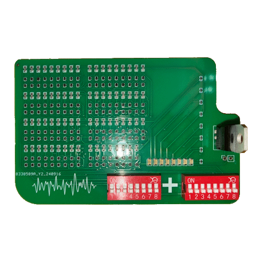
It's a series of eight full adders, made using NMOS NAND gates to
optimize the part count. I found a random schematic someone had made
for a full adder made from NAND gates and that was basically it. The
"hardest" part of the project was arranging the parts on the PCB and
routing them, and I used an auto routing plugin and my placement was
not great. There were a ton of easily fixable traces that are too
long and I put a voltage regulator for the USB power for
legitimately zero good reasons. I think my original plan was to also
put headers on the board for power? Now it just consumes power and
warms up the board.
I think that this was my first PCB that I ever designed and ordered,
and it's pretty terrible. Surprisingly, other similar projects I
found (Discrete adders, eight bits) used more components and cost
muchmore than what I ended up paying, which I think totaled up to
about thirty-five dollars for five boards, three of them being fully
assembled. Maybe because it's all SMD and I chose the cheapest parts.
If I rub my finger along the rows of transistors, the LEDs start to
light up and flicker randomly. I must have made my pull-up resistor
too small, if that would even fix it. It's still fun to flip the
board and look at the insane tangle of traces the autorouter deemed
most efficient. My placement must have been truly terrible.